

Semiconductor wafers are the building blocks of modern electronics, serving as the foundation for integrated circuits (ICs) that power everything from smartphones to supercomputers. The manufacturing process of these wafers is incredibly complex and requires a high level of precision. Semiconductor inspection equipment plays a crucial role in ensuring the quality and reliability of semiconductor wafers. As a leading supplier of Semiconductor Inspection Equipment, I'd like to delve into how this equipment works on semiconductor wafers.
The Importance of Semiconductor Wafer Inspection
Before we dive into the working mechanism, it's essential to understand why semiconductor wafer inspection is so important. Semiconductor wafers are produced through a series of intricate processes, including deposition, lithography, etching, and doping. At each step, there is a risk of defects occurring, such as particles, scratches, or pattern irregularities. These defects can significantly impact the performance and yield of the final semiconductor devices. By detecting and analyzing these defects early in the manufacturing process, semiconductor inspection equipment helps manufacturers identify and correct issues, reducing production costs and improving product quality.
Types of Semiconductor Inspection Equipment
There are several types of semiconductor inspection equipment, each designed to detect different types of defects and perform specific functions. Some of the most common types include:
Automatic Optical Inspection (AOI) Equipment
Automatic Optical Inspection Equipment uses high-resolution cameras and advanced image processing algorithms to inspect semiconductor wafers for surface defects, such as particles, scratches, and pattern defects. AOI systems are fast, non-destructive, and can detect a wide range of defects with high accuracy. They are typically used in the front-end of the semiconductor manufacturing process to inspect wafers after lithography and etching steps.
Scanning Electron Microscopy (SEM) Equipment
SEM equipment uses a focused beam of electrons to scan the surface of a semiconductor wafer and generate high-resolution images. SEM can provide detailed information about the size, shape, and composition of defects, making it a powerful tool for defect analysis. However, SEM is a relatively slow and expensive inspection method, and it requires a vacuum environment, which limits its use in high-volume production.
Atomic Force Microscopy (AFM) Equipment
AFM equipment uses a tiny probe to scan the surface of a semiconductor wafer and measure the forces between the probe and the wafer surface. AFM can provide high-resolution topographical images of the wafer surface, allowing for the detection of nanoscale defects, such as surface roughness and step height variations. AFM is a non-destructive inspection method that can be used in both air and liquid environments, making it suitable for a wide range of applications.
How Semiconductor Inspection Equipment Works
The working principle of semiconductor inspection equipment varies depending on the type of equipment and the specific application. However, most semiconductor inspection equipment follows a similar basic process:
Wafer Loading and Positioning
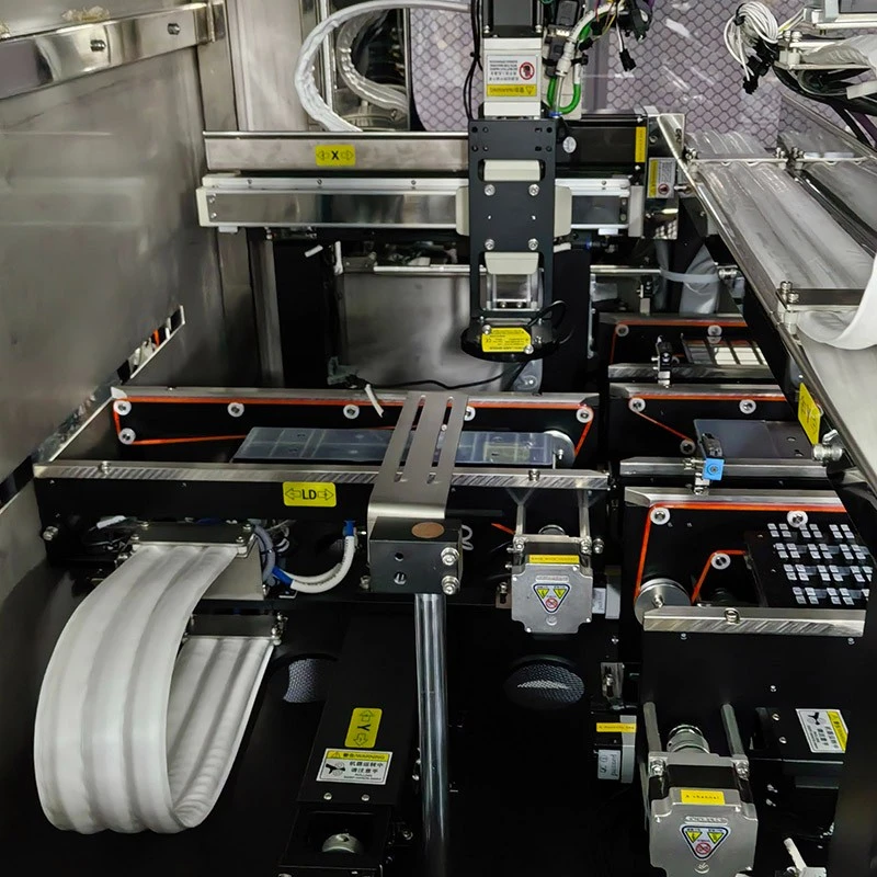
The first step in the inspection process is to load the semiconductor wafer onto the inspection equipment. The wafer is typically placed on a precision stage that can move the wafer in multiple directions to ensure that the entire wafer surface can be inspected. The stage is also equipped with sensors to accurately position the wafer and ensure that it is aligned correctly with the inspection system.
Illumination and Imaging
Once the wafer is loaded and positioned, the inspection equipment illuminates the wafer surface using a light source, such as a laser or a white light. The light reflects off the wafer surface and is captured by a camera or a detector. The camera or detector converts the light into an electrical signal, which is then processed by the inspection system to generate an image of the wafer surface.
Defect Detection and Analysis
The next step is to analyze the image of the wafer surface to detect and classify defects. The inspection system uses advanced image processing algorithms to compare the image of the wafer surface with a reference image or a pre-defined pattern. Any deviations from the reference image or pattern are identified as potential defects. The inspection system then analyzes the size, shape, and location of the defects to determine their severity and classify them into different categories, such as particles, scratches, or pattern defects.
Data Storage and Reporting
Once the defects are detected and analyzed, the inspection system stores the defect data in a database for further analysis and reporting. The defect data can be used to track the defect rate over time, identify trends and patterns, and optimize the manufacturing process. The inspection system can also generate reports that summarize the inspection results, including the number and type of defects detected, the defect density, and the location of the defects on the wafer surface.
Applications of Semiconductor Inspection Equipment
Semiconductor inspection equipment is used in a wide range of applications throughout the semiconductor manufacturing process. Some of the most common applications include:
Front-End Inspection
In the front-end of the semiconductor manufacturing process, semiconductor inspection equipment is used to inspect wafers after lithography and etching steps to detect and correct defects before they are transferred to the next process step. Front-end inspection helps to ensure the quality and yield of the final semiconductor devices.
Back-End Inspection
In the back-end of the semiconductor manufacturing process, semiconductor inspection equipment is used to inspect packaged semiconductor devices to detect and correct defects before they are shipped to customers. Back-end inspection helps to ensure the reliability and performance of the final semiconductor products.

Process Monitoring and Control
Semiconductor inspection equipment is also used for process monitoring and control to ensure that the semiconductor manufacturing process is operating within the specified parameters. By monitoring the defect rate and other process parameters, semiconductor inspection equipment can help to identify and correct process variations and optimize the manufacturing process.
Advancements in Semiconductor Inspection Equipment
The semiconductor industry is constantly evolving, and semiconductor inspection equipment is no exception. In recent years, there have been several advancements in semiconductor inspection equipment, including:
Higher Resolution and Sensitivity
Advancements in imaging technology and image processing algorithms have enabled semiconductor inspection equipment to achieve higher resolution and sensitivity, allowing for the detection of smaller and more subtle defects.
Faster Inspection Speeds
Advancements in hardware and software technology have also enabled semiconductor inspection equipment to achieve faster inspection speeds, allowing for higher throughput and increased productivity.
Integration with Other Manufacturing Equipment
Semiconductor inspection equipment is increasingly being integrated with other manufacturing equipment, such as lithography tools and etching equipment, to enable real-time process monitoring and control. This integration allows for the detection and correction of defects as they occur, reducing production costs and improving product quality.
Conclusion
Semiconductor inspection equipment plays a crucial role in ensuring the quality and reliability of semiconductor wafers. By detecting and analyzing defects early in the manufacturing process, semiconductor inspection equipment helps manufacturers identify and correct issues, reducing production costs and improving product quality. As a leading supplier of Semiconductor Inspection Equipment, we are committed to providing our customers with the latest and most advanced inspection technology to meet their evolving needs. If you are interested in learning more about our semiconductor inspection equipment or would like to discuss your specific requirements, please contact us to start a procurement negotiation.
References
- Smith, J. (2020). Semiconductor Manufacturing Technology. Wiley.
- Jones, A. (2019). Introduction to Semiconductor Inspection and Metrology. Springer.
- Brown, R. (2018). Advanced Image Processing for Semiconductor Inspection. IEEE Press.