

Semiconductor inspection equipment plays a pivotal role in the modern communication industry, significantly enhancing the performance of semiconductor products. As a leading semiconductor inspection equipment provider, we understand the intricacies of this process and its far - reaching implications for communication technologies.
The Significance of Semiconductor Inspection in the Communication Industry
In the communication industry, semiconductor products are the backbone of various devices, from smartphones and tablets to base stations and satellite communication systems. The performance of these semiconductor components directly impacts the speed, reliability, and functionality of communication devices. Semiconductor inspection equipment is essential for ensuring that these components meet the high - quality standards required for seamless communication.
One of the primary challenges in semiconductor manufacturing is the presence of defects. These defects can occur at various stages of the manufacturing process, such as during wafer fabrication, packaging, or assembly. Even the smallest defect can lead to significant performance degradation in communication devices. For example, a single short - circuit in a semiconductor chip can cause a mobile phone to experience frequent crashes or a base station to have reduced signal strength.
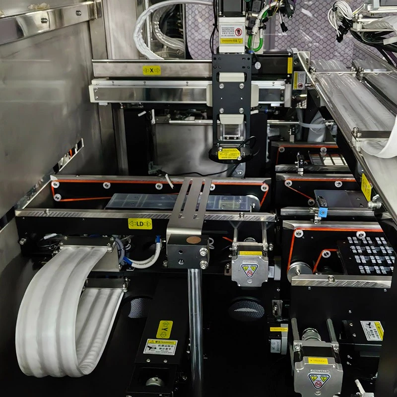
Semiconductor inspection equipment helps in detecting these defects early in the manufacturing process. By using advanced imaging and sensing technologies, our inspection machines can identify defects at the microscopic level. This early detection allows manufacturers to take corrective actions, such as reworking or discarding defective components, before they are integrated into final products.
How Semiconductor Inspection Equipment Improves Performance
1. Quality Assurance
Our semiconductor inspection equipment provides comprehensive quality assurance for semiconductor products. It can inspect various parameters, including dimensional accuracy, surface defects, and electrical properties. For instance, in the case of PCB (Printed Circuit Board) manufacturing, our Pcb Visual Inspection Machine can detect issues such as broken traces, misaligned holes, and solder defects. By ensuring the quality of PCBs, which are crucial components in communication devices, we help improve the overall performance and reliability of these devices.
The inspection process is highly automated, which reduces the risk of human error. Our machines are programmed to follow strict inspection criteria, ensuring consistent and accurate results. This level of quality control is essential in the communication industry, where even minor variations in semiconductor performance can have a significant impact on device functionality.
2. Yield Improvement
Yield improvement is another critical aspect of semiconductor manufacturing. By detecting and eliminating defective components early in the process, our inspection equipment helps increase the yield of high - quality semiconductor products. In the communication industry, where the demand for high - performance devices is constantly growing, improving yield is essential for meeting market needs.
For example, our CCD Visual Inspection Labeling Machine can quickly identify defective semiconductor chips during the packaging process. By removing these defective chips, manufacturers can focus their resources on producing and testing good - quality chips. This not only reduces waste but also increases the overall productivity of the manufacturing process. Higher yields mean that more high - performance semiconductor products can be produced, which in turn can be used to improve the performance of communication devices.
3. Performance Optimization
Semiconductor inspection equipment also plays a role in performance optimization. Our machines can analyze the electrical and physical properties of semiconductor components to ensure that they meet the desired performance specifications. For example, in the case of Mini LED displays, which are widely used in high - end communication devices such as smartphones and laptops, our Mini LED Automated Optical Inspection Machine can detect issues such as uneven brightness, color deviation, and dead pixels.
By optimizing the performance of Mini LED displays, we can enhance the visual experience of communication device users. Additionally, for semiconductor chips used in communication systems, our inspection equipment can test parameters such as signal processing speed, power consumption, and noise levels. By ensuring that these parameters are within the specified range, we help improve the performance of communication devices in terms of data transfer speed, battery life, and signal quality.
Advanced Technologies in Semiconductor Inspection
Our semiconductor inspection equipment incorporates advanced technologies to provide accurate and efficient inspection results. Some of the key technologies include:
1. Optical Inspection
Optical inspection is one of the most widely used techniques in semiconductor inspection. Our machines use high - resolution cameras and advanced lighting systems to capture detailed images of semiconductor components. These images are then analyzed using sophisticated algorithms to detect defects. Optical inspection is non - destructive, which means that it does not damage the components being inspected. This is particularly important in the communication industry, where semiconductor components are often delicate and expensive.
2. X - ray Inspection
X - ray inspection is used to inspect internal structures of semiconductor components. It can detect hidden defects, such as cracks inside the chip or misaligned internal connections. Our X - ray inspection machines are capable of providing detailed 3D images of semiconductor components, allowing for accurate defect detection and analysis.
3. Electrical Testing
Electrical testing is essential for evaluating the electrical properties of semiconductor components. Our inspection equipment can perform a variety of electrical tests, such as resistance measurement, capacitance testing, and voltage testing. By measuring these electrical parameters, we can ensure that semiconductor components are functioning correctly and meet the required performance standards.

Case Studies
To illustrate the impact of our semiconductor inspection equipment on the communication industry, let's look at some case studies.
Case Study 1: Smartphone Manufacturer
A leading smartphone manufacturer was facing issues with high failure rates in their devices. After implementing our semiconductor inspection equipment, they were able to identify and eliminate a significant number of defective components during the manufacturing process. This led to a substantial reduction in device failure rates, improving the overall quality and reliability of their smartphones. As a result, customer satisfaction increased, and the manufacturer was able to gain a competitive edge in the market.
Case Study 2: Base Station Manufacturer
A base station manufacturer was experiencing problems with signal interference and reduced coverage in their products. Our inspection equipment helped them identify issues with the semiconductor chips used in the base stations, such as high - frequency noise and poor signal processing capabilities. By replacing defective chips and optimizing the manufacturing process, the manufacturer was able to improve the performance of their base stations, resulting in better signal quality and wider coverage.
Conclusion
In conclusion, semiconductor inspection equipment is an indispensable tool for improving the performance of semiconductor products in the communication industry. Through quality assurance, yield improvement, and performance optimization, our inspection machines help ensure that semiconductor components meet the high - quality standards required for modern communication devices.
As a semiconductor inspection equipment supplier, we are committed to providing the latest and most advanced inspection solutions. Our state - of - the - art machines, combined with our expertise in semiconductor inspection, enable us to meet the diverse needs of the communication industry.
If you are a manufacturer in the communication industry looking to improve the performance and quality of your semiconductor products, we invite you to contact us for a detailed discussion on how our inspection equipment can benefit your business. We are ready to provide customized solutions and support to help you achieve your manufacturing goals.
References
- Smith, J. (2020). Semiconductor Manufacturing Technology. New York: Wiley.
- Jones, A. (2021). Advanced Inspection Techniques in the Semiconductor Industry. London: Elsevier.
- Brown, C. (2019). The Role of Semiconductors in Communication Technologies. Tokyo: Springer.